Cleanrooms for
the microelectronics industry
The microelectronics industry imposes some of the strictest environmental control requirements. The ongoing miniaturization of integrated circuits—with technologies now reaching the nanometer scale—has made contamination management a central factor in production quality and economic efficiency.
In this sector, environmental control directly influences failure rates and the financial viability of production. Losses associated with contamination run into the millions of dollars, justifying significant investments in high-precision equipment.
Quick Navigation
Particle Cleanliness Requirements
The microelectronics industry routinely operates within the most stringent classifications of the ISO 14644-1 standard. The manufacture of advanced integrated circuits generally requires ISO 4 or ISO 5 environments, and sometimes ISO 3 for certain specialized applications.
These classifications define the maximum number of particles per cubic meter. For ISO 5, the limit is 100,000 particles of 0.1 microns or larger. For ISO 4, this limit drops to 10,000 particles. This seemingly minor difference has major implications for the design of filtration and air circulation systems.
In practical terms, achieving ISO 4 requires 300 to 540 air changes per hour, compared to 60–90 for ISO 7. Ceiling filtration coverage can range from 50 to 90% of the total surface area, compared to 15 to 30% for less stringent classifications. These requirements directly influence both initial investment and operating costs.

Three Types of Contamination to Manage
Particulate contamination: The most visible and best understood form. Particles come primarily from people (80% of contamination), materials, and production equipment.
Molecular contamination: Volatile organic compounds, acids, bases, and other reactive molecules can cause failures even at extremely low concentrations. This form of contamination requires specialized monitoring and chemical filtration in addition to particulate filtration.
Static electricity: Electrostatic discharges damage sensitive electronic components. Electrostatic attraction also draws particles toward surfaces, exacerbating particulate contamination.
Technological Advancements and Flexibility
Production lines in microelectronics are evolving rapidly. Technologies and processes are updated every 2 to 3 years. This reality requires careful consideration of architectural flexibility from the initial design phase—the ability to reorganize, infrastructure scaled to accommodate additional equipment, and modular systems that allow for modifications without disrupting adjacent areas.
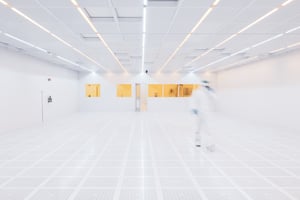
To achieve ISO Class 3 through ISO Class 5 cleanroom classifications, the design typically relies on raised floors combined with vertical airflow. Filtered air passes through the ceiling, descends through the work area, and then returns via perforated panels in the floor to a return plenum.
This approach offers several advantages. The unidirectional airflow prevents turbulence that would resuspend particles. Raised floors also allow utilities—electricity, data, and plumbing—to be housed beneath the work surface, making the infrastructure accessible without disrupting operations.
The typical height of the plenum ranges from 45 to 60 cm. The distance between the ceiling-mounted filtration units and the air returns should generally not exceed 3 meters to maintain a uniform airflow.


Controlling static electricity requires an integrated approach that combines materials, active systems, and operational protocols.
Conductive and dissipative materials: Floors have a controlled resistance between 10⁶ and 10⁹ ohms—conductive enough to dissipate charges, yet resistive enough to prevent electrical arcing.
Air ionization: Ionization systems generate positive and negative ions that neutralize charges in the ambient air. These systems are particularly important in areas where silicon wafers and lithography masks are handled.
Grounding: All equipment, surfaces, and personnel are connected to a common grounding system.
Certain manufacturing processes, particularly photolithography, use resins that are sensitive to ultraviolet and blue light (200 to 500 nanometers). Even brief exposure to these wavelengths can trigger undesirable chemical reactions.
Photolithography rooms therefore use filtered lighting that emits primarily in the yellow wavelength range (570–620 nanometers). This light allows operators to work normally while protecting the photosensitive materials.
This requirement influences the architectural design: windows with specialized yellow films, adapted lighting fixtures, and physical separation of photolithography areas from other production spaces.


In addition to particulate control, certain applications require control of molecular contaminants. These molecules originate from solvents, equipment, or even the outgassing of construction materials.
The control strategy combines several approaches: rigorous selection of low-emission building materials, chemical filtration using activated carbon or potassium permanganate, and monitoring when processes require it.
All materials used in critical rooms can be tested for their outgassing rates. Materials that emit significant amounts of volatile compounds are avoided in the most sensitive environments.
The rapid pace of technological change influences our architectural choices. We prioritize systems that allow for reorganization without affecting adjacent areas. The infrastructure is often designed with a 20- to 30-percent margin to accommodate future expansion and the addition of equipment that consumes more energy.
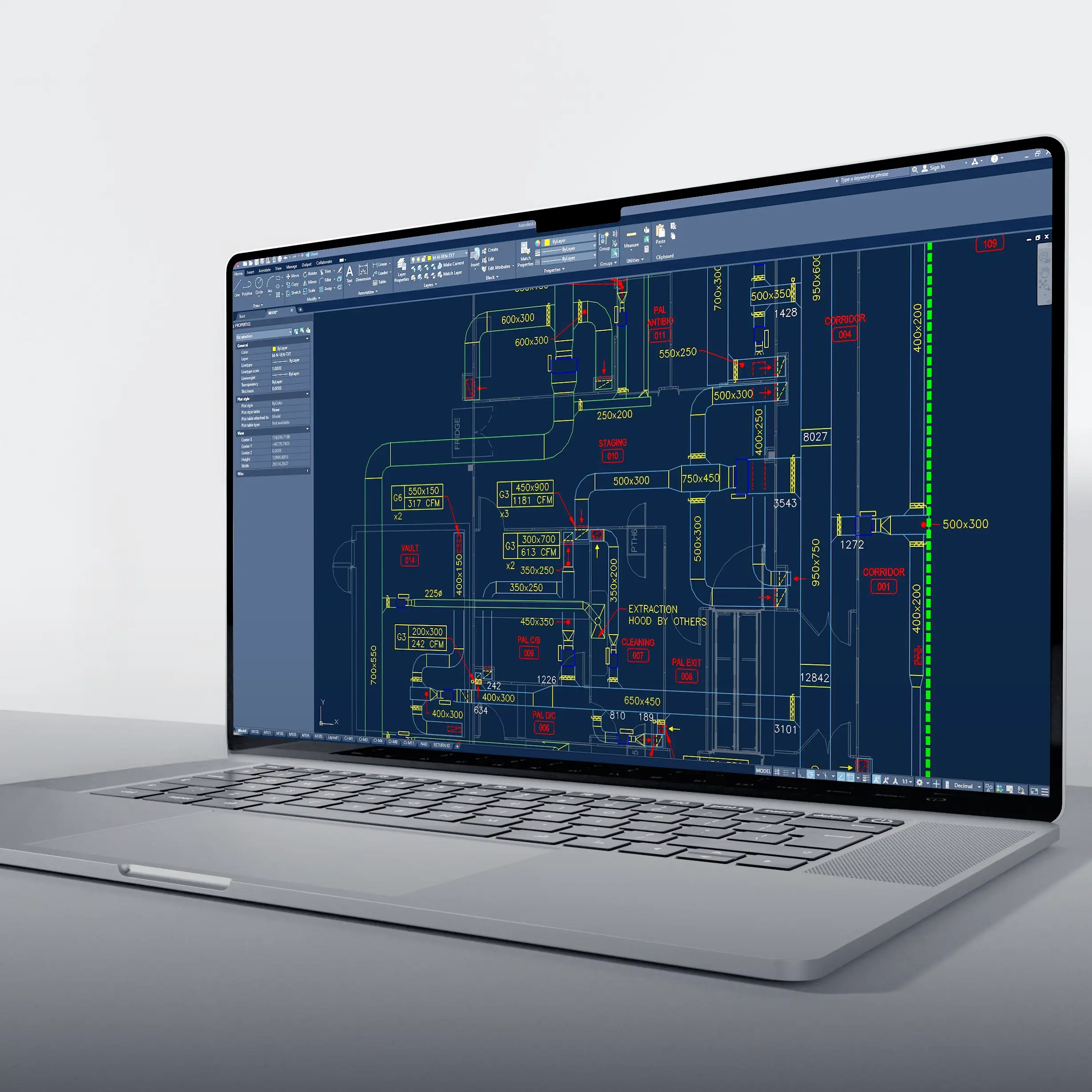
Utilities are generally routed beneath the raised floor, allowing for reconfigurations without major reconstruction. Walls and partitions can be repositioned according to changing needs while maintaining the required classifications.

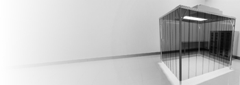
Our experience in microelectronics spans a range of classifications—from ISO 3–4 environments for advanced applications to ISO 6–7 environments for less critical applications, including the integration of cost-optimized mini-environments that maintain adequate protection. Whether you’re planning a new facility, a capacity expansion, or an upgrade to existing equipment, our approach is to understand your specific needs and then design solutions that balance technical performance with budgetary constraints.
THE CONSAB DIFFERENCE
Our strength lies in our ability to offer you unparalleled consulting services thanks to our:
Independence from manufacturers:
Recommendations based on your actual needs, budget, timelines, and technical requirements—not on a pre-determined catalog.
Integrated design-build expertise:
The ability to manage both design and construction, allowing us to anticipate on-site challenges as early as the consultation phase—helping you avoid surprises, delays, and additional costs.
Agile and personalized approach:
We offer either full-service management of your project or a more targeted approach for a specific phase.
Ready to bring your microelectronics cleanroom project to life?
Whether you’re planning a new facility, a capacity expansion, or an upgrade to existing equipment, our team has the technical expertise to support you from initial design through final qualification.